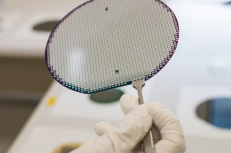
Microfabrications
Fully equipped cleanroom for microfabrication: electronic device, thin film coating, surface patterning.
High flexibiliy and customization
Maximum wafer diameter: 6”
Cleanroom space rental
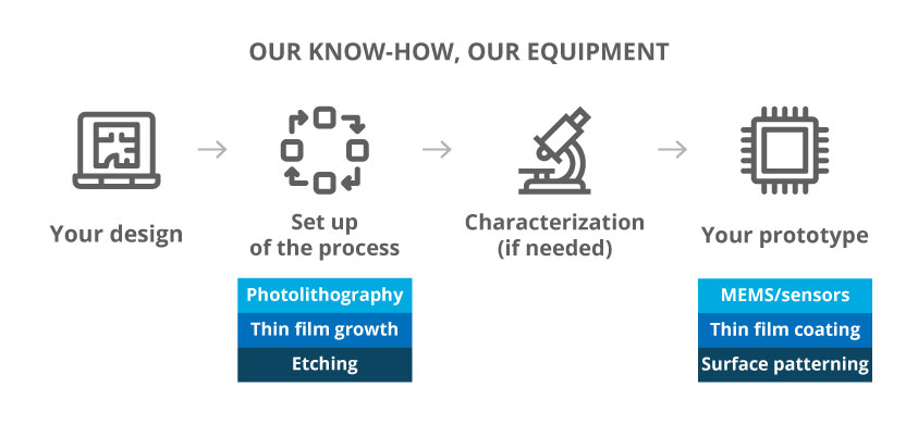
Our know-how, our equipment
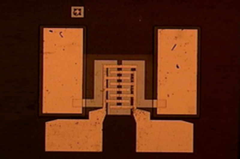
Mems and sensors
In our cleanroom complex microstructures can be realized.
We provide photolithographic process, thin film deposition and dry/wet etching.
We perform the whole process (from silicon wafer to device) or single technological step.
Any need will be processed with the most appropriate technique
Thin Film coating
Deposition methods
- Thermal evaporation
- E-beam
- DC e RF Magnetron Sputtering
- Reactive Magnetron Sputtering
Coatings
- Metals (Al, Cu, Ni, Cr, Ti, Sn, Mo, etc.)
- Precious metals (Au, Ag, Pt)
- Semiconductors (Si, Ge)
- Oxides (SiO2, TiO2, Ta2O5, Al2O2, etc.)
- Hard coatings (SiC, WC, etc.)
Substrate
- Silicon, Metals, Plastics, Glass, Optical fiber…
- We are open to test different material and substrate
Surface patterning
We customizes surface micro- and nano- patterning for different application
e.g. superhydrophobicity, self-cleaning, antifog, antimicrobial, biosensing…
We will find the best strategy to get the required morphology effects:
- subtractive techniques (etching)
- additive techniques (depositing particles on the surface)
- soft lithography
- surface structure can be coupled with chemical functionalization
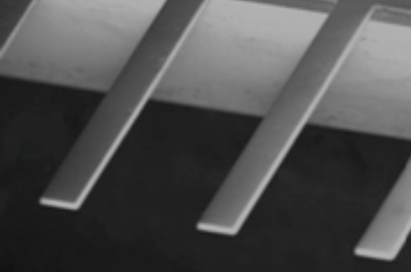
Case study
Aim of the project
We demonstrate the feasibility of a deep through etch for the realization of a sensor for aerospace applications.
Challenges
- passing through etch on 525m silicon
- high verticality of the etched walls
Results
DRIE (Deep Reactive Ion Etching) process have been calibrated especially for this application.

REGISTERED OFFICE
Piazza Solferino, 20
10121 Torino
P.I. 11541890015